- Home
- Who We Are
- What We Do
- Industry Applications
- Circular Economy
- Media
- Information Packs
- Interesting Reads
- Component Preparation for Mission-Critical Applications
- What is Robotic Solder Dip (Retinning, Alloy Conversion, Alloy Refresh)?
- Reballing: What Is It And When Do You Need It?
- The Quiet Deadline: How Obsolescence Shapes Modern Production
- Is Your Supply Chain Safe? Combatting the Threat of Counterfeit Electronic Components
- Quality
- Contact
DECAPSULATION
Exposing semiconductor devices for analysis.
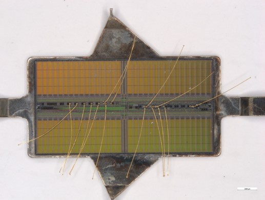
Decapsulation is the removal of a cap, lid, or encapsulating material from a packaged integrated circuit by mechanical, thermal, or chemical means. Techniques should be compatible with the particular packaging configuration to minimise complications from the introduction of foreign matter or damage to the device.
Decapsulation is performed to gain access to the package cavity and/or surface of a device to allow for further analysis. In the case of a hermetic device, removal of the lid permits visual inspection for foreign material, corrosion, mechanical damage, or other workmanship and processing issues. Removal of polymeric encapsulating material from a plastic-packaged part also reveals the IC surface.
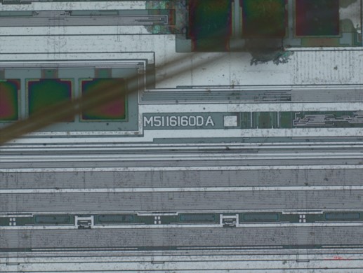
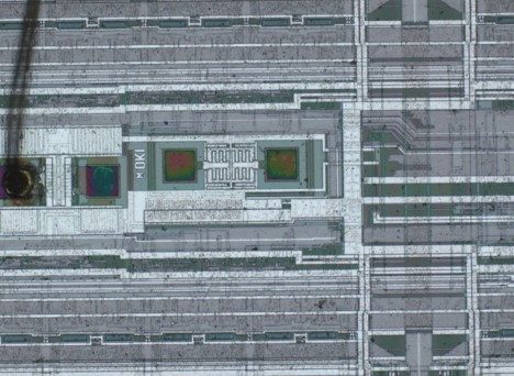
Retronix performs decapsulation of plastic molded packages using an automated etching system. This safe etchback system allows for further investigation at the die level. This technique and method are used to further prove or disprove the authenticity of ICs.
Retronix can also use decapsulation and high magnification analysis to check for signs of damage on the surface of an IC. This could be to check whether the die has been re-assembled or re-packaged or to verify whether a gross functional failure during IC test has been generated by physical damage or overstress.


Contact Us For More Information
© 2024
UK: Retronix, North Caldeen Rd, Coatbridge, Scotland, United Kingdom. ML5 4EF / Email: sales@retronix.com / Phone: +44 (0) 1236 433 345
USA: Retronix Global Inc, 1007 S Heatherwilde Blvd, Ste.300, Pflugerville, TX, 78660 / Email: USA@retronix.com
USA: Retronix, 10560 Dr.M.L.K Jr Street North, St.Petersburg, FL, 33716 / Email:USA@retronix.com

