
High reliability assemblies and the threat of tin whiskers
It’s a well-known fact that Tin Whisker filaments can grow uncontrollably from tin plating. The danger comes when one of these filaments peel away from the tin & connects with an adjacent component thus causing a short.
The most common method to eliminate tin whiskers is to convert the plating from ‘lead-free’ (tin plating) to tin/lead plating. The process is carried out by simply dipping a component’s terminations into tin-lead solder. High Reliability industries are allowed dispensation to use tin/lead solder, as they cannot run the risk of tin whiskers long term.
New components are mostly sold in lead-free form & therefore High Reliability organisations must convert them to tin/lead, a process that has to conform to GEIA Standard.
The problem is that smaller components such as 0402, 0603, and SOT chip capacitors could not be handled in an automated process. Hand-dipping has been the only conversion method, which can be costly, time-consuming, does not meet GEIA Standards & has more potential for inconsistent application. Many manufacturers are rejecting hand dipping & instead are assembling PCBs with lead paste.
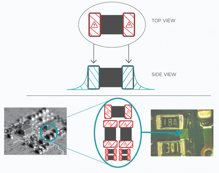
The consequence of this workaround is that the lead solder from the paste only covers the sides of the termination but does not reach the top surface. As widely reported by NASA, the lead paste process DOES NOT protect against the risk of Tin Whiskers.
NASA conducted significant studies on the growth of tin whiskers and field failures. You can access the complete study and presentation clicking here and here
LEAD PASTE FAILINGS
The success of solder dipping as a solution to protect against Tin Whiskers directly depends on coating the exposed tin-plated surface. As components reduce in size, the distance between terminations reduces, increasing the risk of shorts caused by tin whiskers. On densely packed PCBs, there is the additional risk of shorting to adjacent components. Some companies acknowledge this, others ignore it as they have no solution.
A RETRONIX PROCESS FOR SMALL COMPONENTS
With the automated process designed exclusively by Retronix to tin micro devices such as 0402, 0603, SOT’s to GEIA standards, the industry now has a comprehensive all-inclusive solution for tinning requirements.
The Retronix auto tinning process has achieved a significant breakthrough in the electronics industry, particularly in chip component tinning to GEIA standards. Previously, due to their small size, components like capacitors and resistors were not suitable for auto tinning as they were too challenging to process. This puts Retronix in a unique position where they can process all components from lead-free to tin/lead in compliance with the GEIA standard, offering a comprehensive solution to their customers
Retronix unveils comprehensive tinning service: Full BoM conversion to GEIA standards now includes chip components, resistors, SOT’s .. and more.